簡介
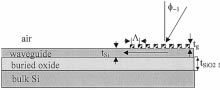
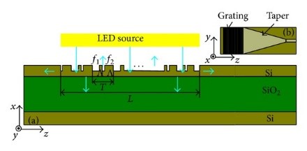
常規矽基絕緣平臺上的光柵耦合器
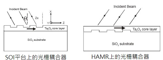
用於熱輔助磁記錄(GAMR)的光柵耦合器
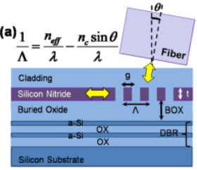
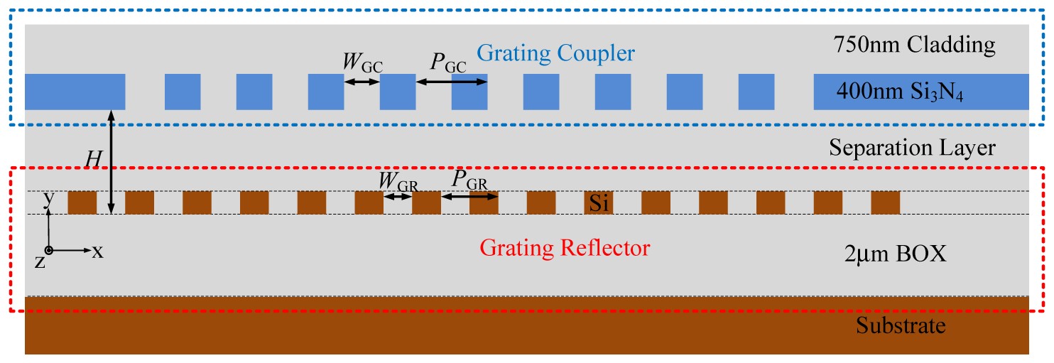
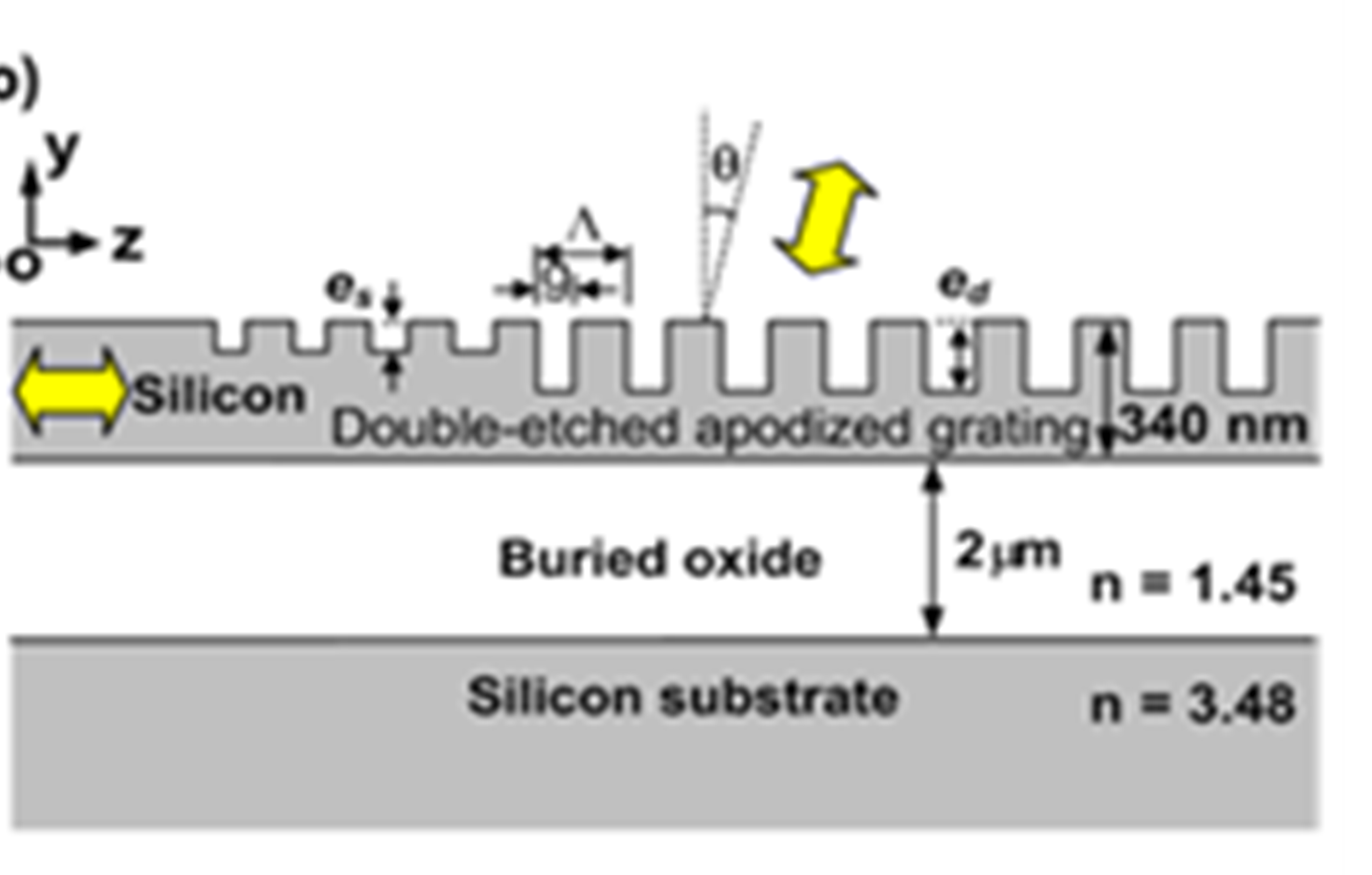
分散式布拉格反射器(DBR)光柵耦合器及光柵反射器
二元閃耀光柵耦合器及雙刻蝕切址光柵耦合器
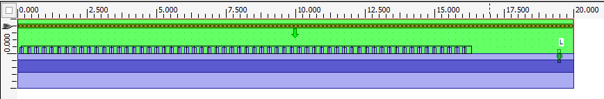
2D FDTD模擬
光柵耦合器設計佈局圖
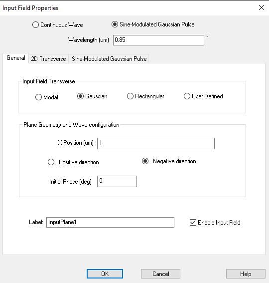
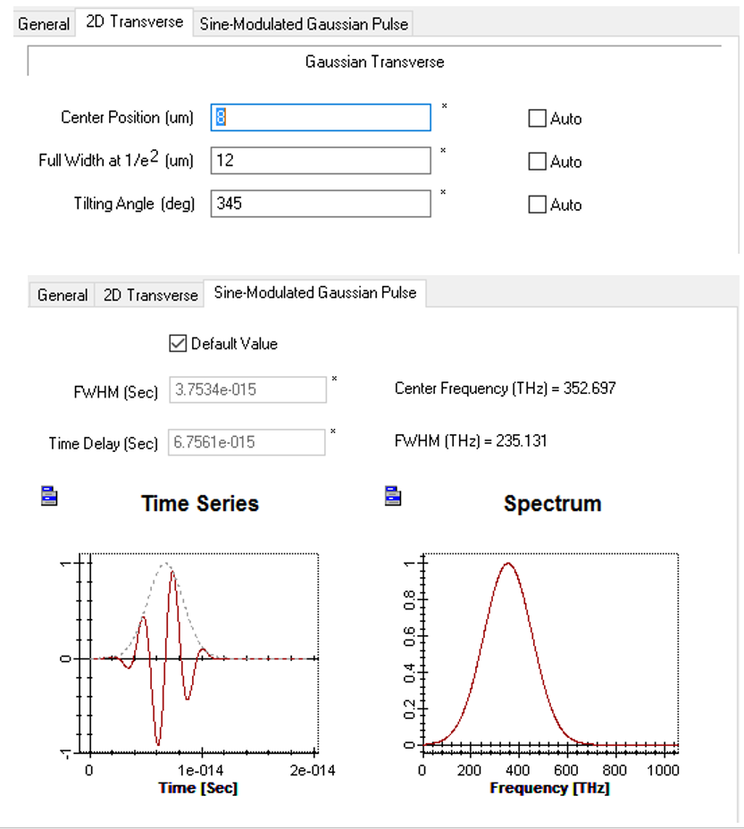
正弦調製高斯脈衝光場設置
模擬結果
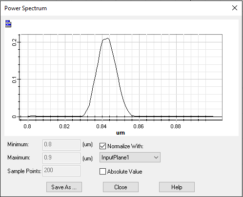
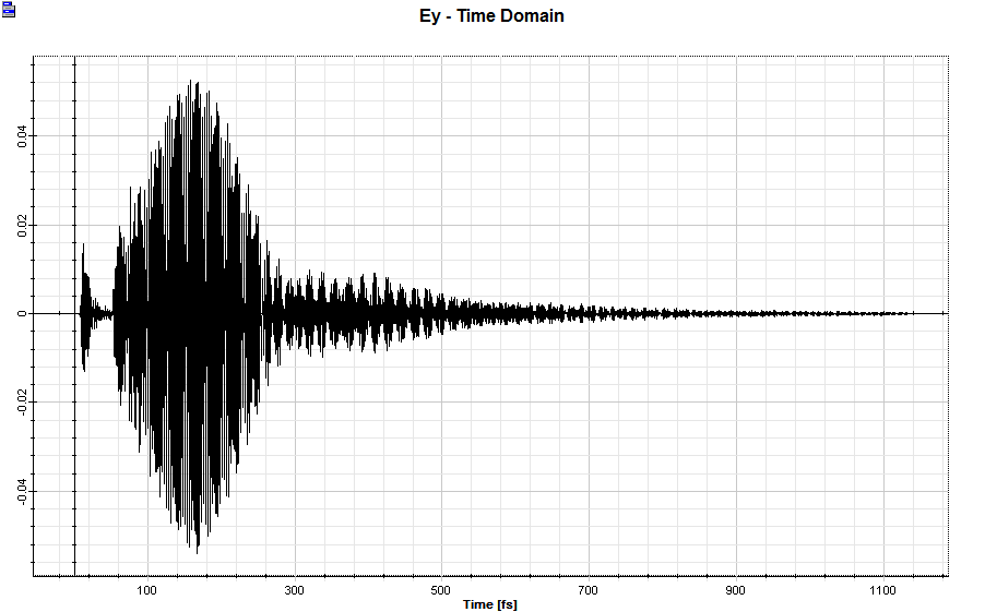
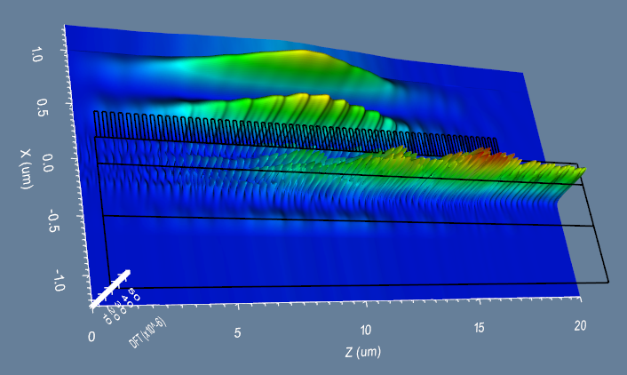
基於線探測器所獲得的功率譜及點探測器所獲得得時域內Ey場
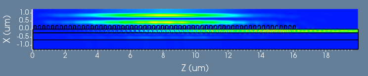
應用區域探測器獲得Ey方向的場強分佈(0.843um)(2D&3D)
參考文獻:
[1] S. M. Csutak, et al., “CMOS-Compatible Planar Silicon Waveguide-Grating-Coupler Photodetectors Fabricated on
Silicon-on-Insulator(SOI)Substrates,” IEEE JQE. VOL. 38, NO. 5, 477-480 (2002);
[2] Chubing Peng, et al., "Input-grating couplers for narrow Gaussian beam: influence of groove depth," Opt. Express 12,
6481-6490 (2004);
[3] Huijuan Zhang, et al., "Efficient silicon nitride grating coupler with distributed Bragg reflectors," Opt. Express 22,
21800-21805 (2014);
[4] Jinghui Zou, et al., "Ultra efficient silicon nitride grating coupler with bottom grating reflector," Opt. Express 23,
26305-26312 (2015);
[5] Li, H., et al. “ Large-area binary blazed grating coupler between nanophotonic waveguide and LED ,” The Scientific
World Journal, 1-6 (2014);
[6] Chao Li, et al. "CMOS-compatible high efficiency double-etched apodized waveguide grating coupler," Opt. Express 21,
7868-7874 (2013);
|